
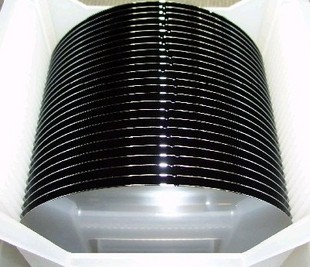
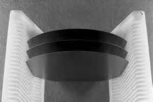
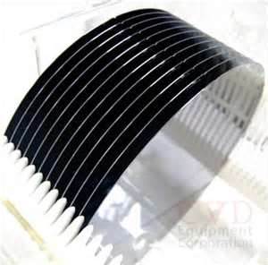
直拉单晶硅片 抛光硅片
我们生产加工高质量直拉抛光硅片
直拉抛光硅片规格
| Grade(等级) | Dimeter(直径) | Type/dopant(类型/掺杂) | Orientaion (晶向) | Thickness (厚度) | Resistivity (电阻率) | Flat |
Surface/Roughness (表面粗糙度) | Geometric parameter |
|---|---|---|---|---|---|---|---|---|
| 最优级(Prime) | 25.4mm 50.8mm 76.5mm | P(Boron) N(Phos/As/Sb) | <100> <111> or special orientation |
400um+/-20 400um+/- 20 400um+/-20 | 0.0001 - 200 Ohm-cm /Customization |
N/A 16mm 22.5mm | polished/etched polished/polished | TTV < 5um TIR <3um STIR < 2um BOW < 20um Warp < 30um Ra<0.5nm |
| 100mm 125mm 150mm | P(Boron) N(Phos/As/Sb) | <100> <111> or special orientation | 525um+/-20 625um+/-20 625um+/-20 | 0.0001 - 200 Ohm-cm /Customization | 32.5mm 42.5mm 57.5mm | polished/etched polished/polished | TTV < 5um TIR <3um STIR < 2um BOW < 20um Warp < 30um Ra<0.5nm | |
| 200mm | P(Boron) N(Phos/As/Sb) | <100> <111> or special orientation | 725um+/-20 | 0.0001 - 200 Ohm-cm /Customization | nothch/flat | polished/etched polished/polished | TTV < 5um TIR <3um STIR < 2um BOW < 20um Warp < 30um Ra<0.5nm | |
| 300mm | P(Boron) N(Phos/As/Sb) | <100> <111> or special orientation | 775um+/-20 | 0.0001 - 200 Ohm-cm /Customization | notch/flat | polished/etched polished/polished | TTV < 5um TIR <3um STIR < 2um BOW < 20um Warp < 30um Ra<0.5nm | |
| 控片挡片(Dummy) | 25.4mm 50.8mm 76.5mm | P(Boron) N(Phos/As/Sb) | <100> <111> or special orientation |
400um+/-20 400um+/- 20 400um+/-20 | 0.0001 - 200 Ohm-cm /Customization |
N/A 16mm 22.5mm | polished/etched polished/polished | TTV < 5um TIR <3um STIR < 2um BOW < 20um Warp < 30um Ra<0.5nm |
| 100mm 125mm 150mm | P(Boron) N(Phos/As/Sb) | <100> <111> or special orientation | 525um+/-20 625um+/-20 625um+/-20 | 0.0001 - 200 Ohm-cm /Customization | 32.5mm 42.5mm 57.5mm | polished/etched polished/polished | TTV < 5um TIR <3um STIR < 2um BOW < 20um Warp < 30um Ra<0.5nm | |
| 200mm | P(Boron) N(Phos/As/Sb) | <100> <111> or special orientation | 725um+/-20 | 0.0001 - 200 Ohm-cm /Customization | nothch/flat | polished/etched polished/polished | TTV < 5um TIR <3um STIR < 2um BOW < 20um Warp < 30um Ra<0.5nm | |
| 300mm | P(Boron) N(Phos/As/Sb) | <100> <111> or special orientation | 775um+/-20 | 0.0001 - 200 Ohm-cm /Customization | notch/flat | polished/etched polished/polished | TTV < 5um TIR <3um STIR < 2um BOW < 20um Warp < 30um Ra<0.5nm | |
| extra thick wafer | 25.4mm 50.8mm 76.5mm | P(Boron) N(Phos/As/Sb) | <100> <111> or special orientation |
>1000um+/-20 customization | 0.0001 - 200 Ohm-cm /Customization |
N/A 16mm 22.5mm | polished/etched polished/polished | TTV < 5um TIR <3um STIR < 2um BOW < 20um Warp < 30um Ra<0.5nm |
| 100mm 125mm 150mm | P(Boron) N(Phos/As/Sb) | <100> <111> or special orientation | >1000um+/-20 customization | 0.0001 - 200 Ohm-cm /Customization | 32.5mm 42.5mm 57.5mm | polished/etched polished/polished | TTV < 5um TIR <3um STIR < 2um BOW < 20um Warp < 30um Ra<0.5nm | |
| 200mm | P(Boron) N(Phos/As/Sb) | <100> <111> or special orientation | >1000um+/-20 customization | 0.0001 - 200 Ohm-cm /Customization | notch/flat | polished/etched polished/polished | TTV < 5um TIR <3um STIR < 2um BOW < 20um Warp < 30um Ra<0.5nm | |
| 300mm | P(Boron) N(Phos/As/Sb) | <100> <111> or special orientation | >2000um+/-20 customization | 0.0001 - 200 Ohm-cm /Customization | notch/flat | polished/etched polished/polished | TTV < 5um TIR <3um STIR < 2um BOW < 20um Warp < 30um Ra<0.5nm | |
| extra thin wafer | 25.4mm 50.8mm 76.5mm | P(Boron) N(Phos/As/Sb) | <100> <111> or special orientation |
100um 200um customization | 0.0001 - 200 Ohm-cm /Customization |
N/A 16mm 22.5mm | polished/etched polished/polished | TTV < 5um TIR <3um STIR < 2um BOW < 20um Warp < 30um Ra<0.5nm |
| 100mm 125mm 150mm | P(Boron) N(Phos/As/Sb) | <100> <111> or special orientation | 100um 200um customization | 0.0001 - 200 Ohm-cm /Customization | 16mm+/-2mm | polished/etched polished/polished | TTV < 5um TIR <3um STIR < 2um BOW < 20um Warp < 30um Ra<0.5nm | |
| 200mm | P(Boron) N(Phos/As/Sb) | <100> <111> or special orientation | 100um 200um customization | 0.0001 - 200 Ohm-cm /Customization | 16mm+/-2mm | polished/etched polished/polished | TTV < 5um TIR <3um STIR < 2um BOW < 20um Warp < 30um Ra<0.5nm | |
| 300mm | P(Boron) N(Phos/As/Sb) | <100> <111> or special orientation | 100um 200um customization | 0.0001 - 200 Ohm-cm /Customization | 16mm+/-2mm | polished/etched polished/polished | TTV < 5um TIR <3um STIR < 2um BOW < 20um Warp < 30um Ra<0.5nm | |
| extra flat wafer | 25.4mm 50.8mm 76.5mm | P(Boron) N(Phos/As/Sb) | <100> <111> or special orientation |
400um+/-20 400um+/- 20 400um+/-20 | 0.0001 - 200 Ohm-cm /Customization |
N/A 16mm 22.5mm | polished/etched polished/polished | TTV < 2um TIR <1um STIR < 1um BOW < 10um Warp < 10um Ra<0.5nm |
| 100mm 125mm 150mm | P(Boron) N(Phos/As/Sb) | <100> <111> or special orientation | 525um+/-20 625um+/-20 625um+/-20 | 0.0001 - 200 Ohm-cm /Customization | 32.5mm 42.5mm 57.5mm | polished/etched polished/polished | TTV < 2um TIR <1um STIR < 1um BOW < 10um Warp < 10um Ra<0.5nm | |
| 200mm | P(Boron) N(Phos/As/Sb) | <100> <111> or special orientation | 725um+/-20 | 0.0001 - 200 Ohm-cm /Customization | nothch/flat | polished/etched polished/polished | TTV < 2um TIR <1um STIR < 1um BOW < 10um Warp < 10um Ra<0.5nm | |
| 300mm | P(Boron) N(Phos/As/Sb) | <100> <111> or special orientation | 775um+/-20 | 0.0001 - 200 Ohm-cm /Customization | notch/flat | polished/etched polished/polished | TTV < 2um TIR <1um STIR < 1um BOW < 10um Warp < 10um Ra<0.5nm |